Creating your own PCB might seem like an intricate, industrial task reserved for specialized factories, but with the right approach and a touch of patience, you can etch your own PCBs at home. This journey, though rewarding, is not without its challenges and considerations.
You can etch a PCB by yourself, in a lab or even at home, through a simple and inexpensive production process. It makes sense when you wish to produce a single or a very small number of boards and want to avoid manufacturing costs. The etching process is therefore effective for a small workshop.
The Art of Subtraction
Etching a PCB is a subtractive method where acid is used to remove unwanted copper from a prefabricated laminate. The process begins with applying a temporary mask that protects parts of the laminate from the acid, leaving behind the desired copper pathways. This method is particularly advantageous for small workshops and DIY enthusiasts who need to produce single or limited quantities of boards without incurring significant manufacturing costs.
Safety First: Navigating the Risks
The allure of creating your own PCBs at home comes with inherent risks. The chemicals involved in the etching process are dangerous and can cause injuries if not handled properly. Before diving into the etching process, equip yourself with essential safety gear: gloves, protection glasses, and an apron. Ensure that you work in a well-ventilated area near an emergency eyewash station, a first aid box, and a phone. Familiarity with the proper use of all equipment and tools is crucial; when in doubt, consult knowledgeable individuals or detailed guides.
The Masking Methods: Crafting Your Blueprint
Creating an effective mask is pivotal to the etching process. Two popular methods are:
1. Direct Toner Transfer:
Step-by-Step: Print your circuit layout using a laser printer on suitable paper, such as glossy magazine pages. Place the printed layout face-down on the laminate and transfer the toner to the copper using an iron. After ironing, soak the laminate in water and carefully scrub away the paper.
Challenges: Achieving the right temperature for the toner transfer is tricky. Too high, and the toner will blur; too low, and it won’t stick. This method is more prone to errors but is cost-effective for producing a single PCB.
2. Photo-resistive Laminates (Recommended):
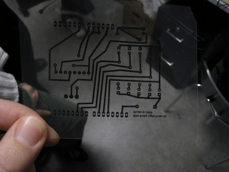
Step-by-Step:
- Print the file in highest resolution, first on white paper, and when satisfied, on a transparent paper or foil. Be careful to set the printer options to NOT “scale to fit”.
- When printing on foil, use either a special toner or a toner dissolver spray to heighten the density and get the print tone overall even.
The spray should be used directly after printing, and care should be taken not to cause any drops. After the toner dries, place the foil in the imaging frame, toner side up. - Peel the protective blue film off the copper laminate (Robo Store) and place it in the imaging frame copper side down, on top of the transparent film. Make sure not to expose the light-sensitive layer to too much light during the development process.
- Close the lid of the imaging frame, set the timer for 4 minutes and press the knob to start the exposure.
- Once the imaging process finishes, place the board in the development tank for 1-2 minutes and shake it once in a while (be careful not to leave it too long, otherwise it will damage the traces).
- Place the board in the rinse tank containing destillated water for a few seconds.
Advantages: Though slightly more expensive, this method offers consistent and high-quality results. The mask template can be reused, making it ideal for producing multiple PCBs.
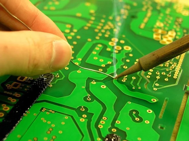
The Etching Process: Dancing with Acid
Choosing the right etching chemicals and equipment can significantly impact the quality and efficiency of the process. Ferric chloride and sodium persulfate are common choices. While a simple plastic box can suffice for etching, using a machine that controls temperature and keeps the fluids in motion will yield better results. Small etching tanks with heating and air pumps, or spray etching machines, can enhance the quality and speed of etching.
To get rid of all unwanted copper follow these etching steps:
- Put the board in the acid tank for about 20 minutes until the copper traces are completely etched. You can tell that it’s finished when the board turns from opaque pink to transparent yellow.
- Move the board into the rinse tank for a few seconds. You can also use an Isopropanol spray.
- Dry the board with a cloth.
The Final Touches: Drilling and Finishing
Once the etching is complete, secure the board to a piece of wood and drill the necessary holes for components, ensuring the holes are slightly larger than the pins or wires. Trim the board to the desired size and consider applying a varnish spray as a finishing coat to protect the traces.
By now, you should be holding a fully functional PCB, a testament to your skill and dedication. This process not only saves costs but also provides a deeper understanding of the intricate world of electronics. While this guide offers a solid starting point, there is always more to learn and refine. So, embrace the challenges, prioritize safety, and enjoy the satisfaction of creating your own shit.


Leave a comment